Today, I will be providing you with some valuable insights into the fascinating world of LED packaging. I understand that this topic might seem a bit dry, but trust me, it holds great significance. So, let's dive right in, shall we?
Now, I have noticed that in the past, customers have had several inquiries regarding LED packaging. If you happen to share some of these doubts, fret not!
What is a LED package?
What is the theory of LEDs?
What is the packaging process of LED?
How big is the LED packaging market?
What are the different LED packages?
What are the different types of SMD LED packages?
What is the difference between LED chip and package?
What is the difference between LED bulb and LED module?
What is the difference between LED chip and package?
Whether you're a lighting designer, a professional lighting purchaser, or simply a passionate lighting enthusiast, understanding the intricacies of LED packaging is essential. You see, LED packaging technology plays a pivotal role in our everyday lighting experiences and directly impacts the quality of the LED chips we use.
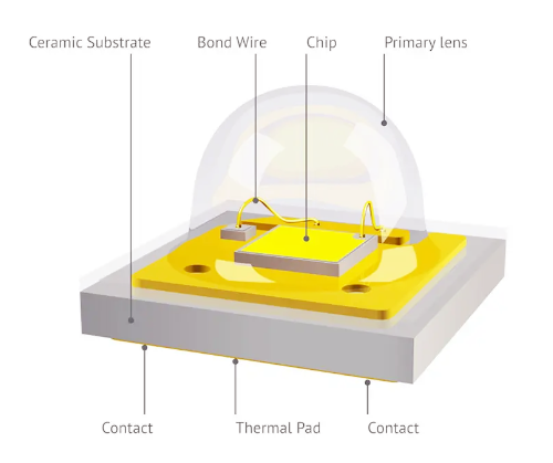
LED packaging encompasses the techniques and processes involved in encapsulating delicate LED chips, protecting them from external elements, and providing optimal thermal management. This packaging not only ensures the durability and reliability of LED products but also influences their overall performance and efficiency.
So, whether you're selecting the perfect lighting fixtures for your design project or seeking high-quality LED products, having a solid grasp of LED packaging will empower you to make informed decisions and achieve the desired lighting outcomes.
LED packaging, unlike integrated circuit packaging, involves the encapsulation of light-emitting chips using plastic or ceramic materials. This process aims to shield the LED chip from external impurities present in the air, which could otherwise corrode the chip circuit and lead to a decline in electrical performance. Moreover, packaging the chip enhances its ease of installation and transportation.
When it comes to LED packaging, it's important to note that it serves a dual purpose. Not only does it safeguard the LED chip, but it also facilitates the transmission of light. Consequently, LED packaging demands specific requirements for packaging materials. It's worth mentioning that the disparity in packaging technologies directly impacts the quality of LEDs.
By employing superior packaging and heat dissipation technologies, LEDs can operate below 60°C, resulting in a lifespan exceeding 50,000 hours. Therefore, a profound understanding of LED packaging becomes paramount for individuals involved in lighting design, procurement, or anyone passionate about the field. This knowledge empowers them to make informed decisions and ensures the desired performance and longevity of LED products.
The role of LED phosphor is of great significance in the world of lighting. Let's delve into its functions and characteristics, shall we?
Phosphor powder, an inorganic compound, plays a crucial role in LED technology. It possesses the unique ability to absorb specific wavelengths of light emitted by LEDs and convert a portion of that energy into visible light with high visual efficiency. This conversion process, known as luminescence, allows phosphors to emit light.
Typically, phosphors absorb blue light emitted by LEDs and transform it into greenish-yellow or red light output. To create fluorescent substances, an activated agent containing element B is added to a suitable compound called the matrix, denoted as A:B. These phosphor particles usually range from sub-micron to tens of microns in size.
LED phosphors can be categorized based on their luminous colors, such as red, green, and blue phosphors. Additionally, they can be classified by their composition, including silicates, chlorosilicates, aluminates, nitrogen oxides, nitrides, tungstates, platinum salts, sulfur oxides, and more. Presently, the most commonly used phosphors in LEDs are silicate or nitrogen oxide green, YAG yellow powder, and nitride red powder.
To achieve white light production, phosphors can be employed in three different ways. The first method involves combining blue LED chips with yellow phosphors. The second method combines blue LED chips with red and green phosphors. Lastly, UV-LED chips can utilize red, green, and blue primary color phosphors. Each approach has its advantages and disadvantages, which are detailed in Table 1-5.
Table 1-5: Comparison of Advantages and Disadvantages of LEDs Producing White Light Using Different Phosphors
|
White Light Generation Method |
Advantages |
Disadvantages |
|
Blue LED with Yellow Phosphor |
Single chip emits white light, low cost, simple production |
Low efficiency, color rendering needs improvement, difficult to achieve low color temperature, light color varies with current, potential for halo effect |
|
Blue LED with Red and Green Phosphors |
Three-wavelength spectrum distribution, good color rendering, adjustable light color and color temperature |
Light color varies with current, potential for halo effect (although less pronounced) |
|
UV-LED with Red, Green, and Blue Phosphors |
Good color rendering, adjustable light color and color temperature, uniform light color with high conversion efficiency |
Difficult powder blending, development of high-efficiency phosphors needed |
When using LED packaging glue, it is crucial to master the proportion of the AB glue. This involves accurately measuring and mixing the epoxy resin with the necessary additives. Stirring the mixture thoroughly is also necessary to ensure a homogeneous blend. By doing so, the ingredients are properly dispersed, leading to optimal curing and adhesive performance.
Furthermore, it is vital to control the curing and aging temperature correctly. Maintaining the recommended temperature range facilitates the complete curing of the AB glue, resulting in the desired bonding strength and stability.
By following these guidelines, the LED packaging glue can be effectively utilized, providing reliable protection and encapsulation for the LED chips.
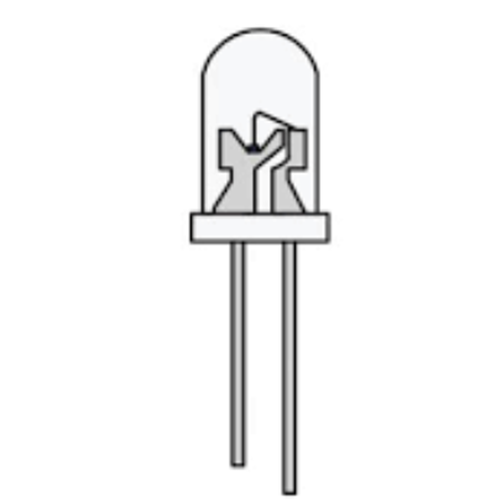
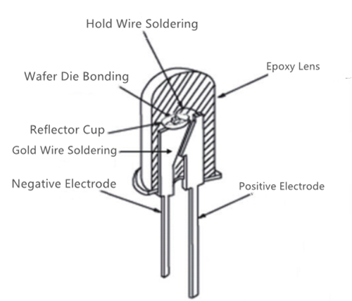
Before 2002, pin-type packaging was the main technology used in LED packaging. The pin-type package is mainly used in φ3-5mm package structure, generally used for small current (20~30mA), low power (less than 0.1W) LED, it uses a lead rack as the pin of various package shapes.
At present, the design of needle shaped LEDs is relatively mature, with a wide variety and high technological maturity. The structure of packaging and reflectors is still in development. Ten years ago, it was recognized as a convenient and economical solution in the lighting industry, but its development is limited by attenuation life, optical matching, and failure rate.
Figure 1-1 shows the large-size ring resin package following the low-power DIP LED package idea.
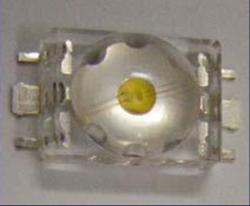
Piranha LED packaging possesses distinct characteristics. The piranha package is square and features a clear resin enclosure with a missing pin at the negative end. The piranha LED is an astigmatic LED, offering a wide luminous angle exceeding 120°. It exhibits exceptionally high luminous intensity and can withstand greater power.
The shape of the piranha encapsulation particle varies, including options such as round heads with diameters of φ3mm and φ5mm, as well as concave and flat head shapes. The selection of different packaging molds can cater to specific requirements for the light angle. Piranha package LEDs excel in heat dissipation, and when compared to ordinary φ5mm LEDs, they experience minimal light decay, resulting in a longer lifespan and cost savings. However, it's worth noting that the piranha package tends to have a slightly larger volume than φ5mm LEDs. Additionally, due to its wide luminous angle, it performs exceptionally well in applications involving full-color RGB mixed lighting, surpassing the performance of straw hat φ5mm LEDs.
Figure 2-1 showcases the piranha epoxy resin package
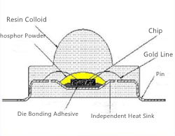
The aluminum substrate (MCPCB) package adopts an aluminum-based printed circuit board package, which can better solve the heat dissipation problem of high-power LED and improve the working stability and reliability of LED. As shown in Figure 3, the bottom cooling window of the LED is directly fixed on the insulation layer by reflow welding, and the three-dimensional long aluminum substrate is directly cooled. The LED is still led by two electrodes and welded together with the circuit layer.
TO(Transisto Out-line), was an early transistor package specification. In recent years, drawing on the idea of high-power transistor packaging, LED products using TO-type packaging have accounted for a certain market share.
The surface mount packaging technology is mainly installed on the component carrier board by melting and resolidifying the solder to form SMD LED products. Such LED products have a great improvement in quality, more convenient integration, and high production efficiency. In recent years, SMD LED has become a hot spot for development, and its application design is flexible, which can solve the problems of luminous intensity, luminous angle, and low overall cost.With a lighter PCB and reflector material, showing that the reflector needs to be filled with less epoxy and the removal of the heavier carbon steel material pins, the product weight can be easily reduced by half by reducing the size, and finally the application is perfect. In particular, the TOP light emitting (TOP) type SMD LED is in continuous development, package support size, package structure design, material selection, optical design, heat dissipation design and other continuous innovation, with great technical potential, so SMD LED has the trend of accelerated development, and will gradually replace pin-type LED.
Although surface-mount packaging technology occupies a certain share of packaging technology and has the trend of accelerating development, the surface mount process needs to use a large number of welding balls and welding paste. Lead tin alloy has always been dominant in solder, but lead and lead compounds are highly toxic substances, which are extremely toxic to humans and livestock and can cause serious pollution. Therefore, the development and use of high-quality and low-cost lead-free solder has become a key to its development.
In the 1990s, domestic power LED packages began to be utilized, primarily focusing on meeting two main requirements. Firstly, the package structure should possess high light efficiency. Secondly, it should aim to minimize thermal resistance, ensuring optimal photoelectric performance and reliability of power LEDs. Power LEDs can be classified into two categories: low-power LEDs and high-power LEDs. Due to the drawbacks of low-power LEDs, such as significant light decay and high installation costs, there has been a shift towards high-power LEDs as the core of future lighting solutions.
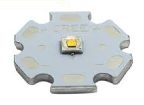
To address the requirements of large LED power consumption, substantial heat output, and high light efficiency, major companies worldwide have invested significantly in the research and development of LED packaging technology. Notably, foreign research results in power-type packaging, such as the 5W series, Luxeon series, and Norlux series products, have gained strong competitiveness in the LED industry.
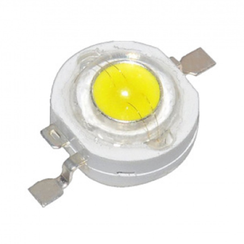
Figure 3 displays Lumen's high-power LED package as an example.
The manufacturing technology for power type large-size chips is still undergoing development. Additionally, the structure, optics, materials, and parameter design of power type LEDs are also evolving, with new designs continually emerging. It is important to note that the packaging methods and materials used for high-power LEDs cannot be simply applied to traditional low-power LEDs. The substantial dissipation power, high heat output, and demand for high light efficiency pose greater requirements for LED packaging technology, packaging equipment, and packaging materials.
The homogeneity of luminescence and heat dissipation of large-size chip packages need to be solved. In order to avoid these problems, the method of small-size chip integration can be used to increase the maximum light flux of a single tube. Small chip technology is relatively mature, the improvement of quantum efficiency in the chip will lead to the reduction of heat generated, the effective current density of the active layer of the chip will increase significantly, and the improvement of the efficiency of a single chip makes multi-chip integrated packaging possible.
Multi-chip integrated packaging is a rapidly developing packaging technology in recent years. It assembles a number of chips on a circuit board to form a multi-chip component, which is the basis for the system-level realization of LED component functions. All the chips are laid out on a flat surface. The wiring in the substrate is arranged in a three-dimensional way.
The thermal aggregation effect of the integrated packaged LED device improves the overall thermal conductivity efficiency of the LED device.
The LED digital tube uses LED as the light-emitting unit.
ceramic leadless chip LEDs are already used in some mobile phones and notebook computers
Contact: Mr. Otis
Phone: +8615815758133
Tel: +8615815758133
Email: Hello@lederlighting.com
Add: No. 1 Gaoxin West Road,High-tech Zone, Jiangmen, Guangdong, China